
PCBs are an integral part of electronic and electromechanical devices. One- or single-layer PCBs are the most basic form of PCBs used in simple electronic devices such as a radio, relays, and lighting systems. Double layer or 2-layer PCBs are just as basic except for some aspects. Single-layer PCBs are used by students and enthusiasts in their projects. These types of PCBs have been used over the years; however, the need for multilayer PCBs arose because of the complex designs and shrinking sizes of electronic devices such as smartphones and tablets. This post discusses the details of 1- and 2-layer PCBs, their design, applications.
A single-layer PCB is absolutely basic and has only one conductor material. In this type of PCB, there is only one layer of the substrate, on one side of the board. One side of this substrate is coated with a thin layer of metal such as copper. After this step, the solder mask is applied, followed by application of the silkscreen layer. Since these are single-sided PCBs all the circuits and components are soldered onto that one side. The board used here may be either rigid or flexible.
These PCBs are basic but cost effective, and are still applicable in relatively simple devices such as calculators, printers, solid state relays, power supply devices, and so on. In fact, you can make this PCB on your own as the design is relatively simple, and the circuit is easy to understand. The components are few and distantly placed, so it is easy to differentiate and identify them. Here is a basic layout of a single-layer PCB:
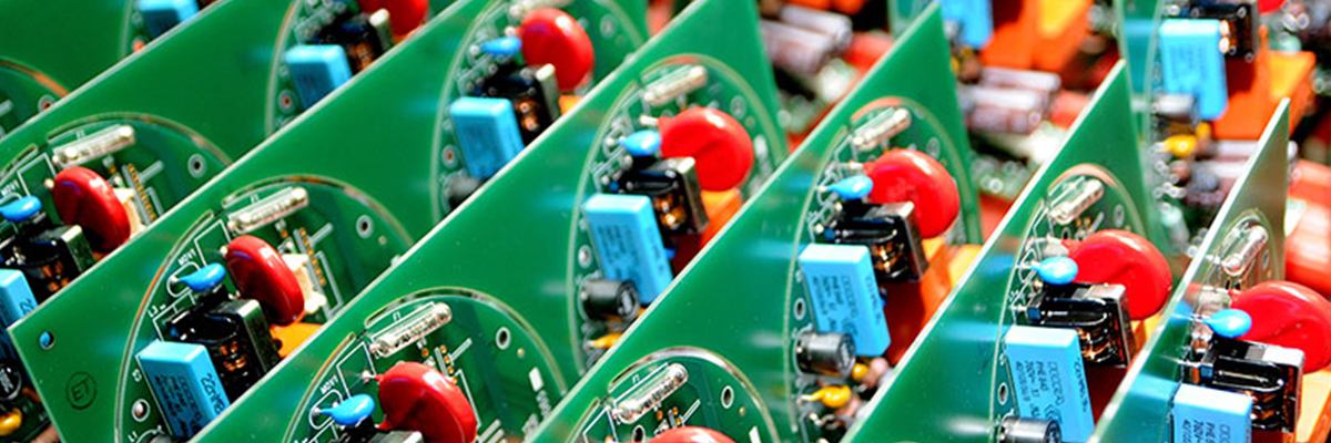
A 2- layer PCB comprises a top and a bottom layer. Electrical connections are done through vias which enable routing for the connection to reach the other end of the board. The base material for this board is usually FR4, aluminum, or even plastic. There is a thin layer of copper laminated to both sides of the board. On top of the copper foil, there is a solder mask layer, which insulates copper from coming into contact with other metals or conductors. A silkscreen layer is applied atop this layer, which has information such as numbering, letters, and symbols for easy understanding. In this type of PCB, the circuits and components are mounted using the thru-hole technology. They may also be surface mounted. Surface mounting offers an advantage in terms of more free space on the board. It also makes the board lightweight as the number of wires running through holes are largely reduced. The board used here may be either rigid or flexible.
A major advantage a 2-layer PCB offers is a larger surface area and layout than 1-layer PCB. Some typical applications of a 2-layer PCB include LEDs, HVAC systems, vehicle dashboards, vending machines, and so on. Here is a basic layout of a double-layer PCB:
If you are looking for PCBs for basic devices or you want to start with electromechanical devices as part of your product line, you can opt for single or double-layer PCBs. It is recommended that you consult an experienced PCB assembler and service provider before deciding upon the PCB design and the number of layers. Twisted Traces is a well-known manufacturer and assembler of various types of PCBs which are RoHS compliant. They have a market presence of over 30 years.
.png)
