
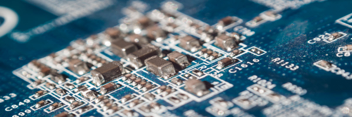
Flexible and rigid-flex printed circuit boards have to meet the requirements of EMI and RF shielding, as these factors may affect their performance. With printed circuit board, being the key power and performance driving component of any electronic device, any flaws induced by EMI and RF may mean big loss in terms of performance. Hence, to avoid this, the PCB manufacturers follow certain EMI and RF shielding methods. This post discusses the effects of EMI and RF and the different methods adopted by manufacturers to avoid them.
Electromagnetic interference (EMI) is a disturbance experienced by an electrical circuit. This disturbance is often generated by an external source by conduction, electrostatic coupling, and induction. This EMI is also known as radio-frequency interference or RFI and it affects the performance of a PCB, sometimes even disrupting its function. The printed circuit boards feature several components that are connected using interconnects. These interconnects would act as an antenna at high frequencies. When this happens, they start emitting EMI, which would impair the performance of the electronic device.
The following are a few factors that help reduce EMI in PCBs.
As discussed above, shielding a PCB requires consideration of several mechanical and electrical design factors in the design and manufacturing phases. You need to partner with experienced PCB manufacturer like Twisted Traces to get them right. The company specializes in PCB assembly and manufacturing and has been serving clients in the medical, municipal, military, and industrial electronics with standard and RoHS PCBs for several years now. You can get in touch with the experts at the company to discuss your requirements.
.png)
