PCB EMI Protection Services
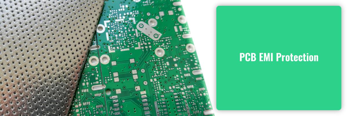
PCB EMI Protection Services
Printed circuit boards (PCBs) are an integral part of electronic devices, and hence they demand accuracy in terms of functioning. Several manufacturing and assembly technologies have emerged in the past few decades, which have tremendously helped PCB manufacturers and assembly service providers improve their accuracy and increase their productivity. However, that is not enough, because designing a quality-driven and performance-oriented PCB is still a big challenge for many of these manufacturers. Among various challenges, electromagnetic interference (EMI) and electromagnetic compatibility (EMC) are two problem areas that PCB engineers have to take care of. To address these, they are offering various PCB EMI protection services. Why are these terms important? How are PCB manufacturers offering PCB EMI protection services to reduce EMI?
Electromagnetic Interference and Electromagnetic Compatibility— How Are They Related?
Electromagnetic interference, also referred to as radio-frequency interference (RFI), is a type of disturbance that may affect the performance of a circuit, sometimes even interfering with the device performance. This disturbance may be brought by an external source, and it may be in the form of electrostatic induction or conduction.
Electromagnetic compatibility is associated with the production, propagation, as well as acceptance of electromagnetic energy in a circuit, which may also interfere with its functioning. This interference may increase when two circuits work in unison, as a part of an application. As the demand for integrated circuits has increased, it is quite obvious that the sources will produce more electromagnetic energy. Owing to all these, it has become important for PCB designers to ensure the EMI and electromagnetic compatibility elements are reduced to a minimum.
Tips to Minimize EMI Issues in a PCB
The following are a few proven design tips that have helped electronic engineers specializing in PCB EMI protection services to minimize EMI issues in a PCB.
-
Identifying and Routing Important Traces: Nowadays, PCBs feature complex designs, and several traces. Among these, it is difficult to identify the ones creating issues. To simplify the issues, most PCB designers concentrate on the traces that enter or leave the printed circuit board. The data lines carrying high-speed signals are one of the main sources of EMI. After identifying these traces, PCB designers can use chips on the printed circuit boards to improve their routing. Improved routing contributes to clean and simpler paths, thereby reducing the EMI.
-
Effective Utilization of the Ground Area: The ground plane of PCB is important, and it helps reduce crosstalk, noise, and emissions. A complex PCB design may require several ground planes, which may later increase the cost of production. This is where PCB designers make an adjustment by dividing the ground planes into three to five different sections, which is later routed into a single largest ground layer. This not only helps reduce the EMI but also keep electromagnetic compatibility in check.
-
Addressing Crosstalk: This is one of the major issues that may aggravate EMI and also affect signal integrity. Crosstalk is caused due to a coupling between two high-speed signal carrying lines. This problem is addressed by separating two traces carrying high-speed signals. The spacing between two high speed lines is always increased such that it is twice the trace width. For instance, if the trace width is 1 mil then the distance is kept to 2 mils or more.
-
Creating a Better Component Segregation: A typical complex PCB may comprise several types of high-speed and low-speed circuits, power supply sections, digital and analog circuits, and so on. For avoiding EMC and EMI, designers group the related areas according to their functionality. They use filters to differentiate the boundaries of subsystems.
-
Increasing Shielding: Nowadays, PCB designers use shields to reduce EMC. These shields are basically conductive materials that are connected to the ground. These shields can reflect as well as absorb the radiation produced by loop antennas. They also help reduce the size of antennas. Thus, they reduce the EMI by attenuating the radiation wave.
Although these are the common practices for designing EMI-free PCBs, designers may also implement other design changes. If you are planning to design EMI-free PCBs for your next project, it is important that you approach reliable PCB assembly service providers like Twisted Traces who offer customized PCB EMI protection services. The company has a vast experience in designing and delivering EMI- and EMC-free PCBs for clients across critical service industries.
.png)

