6 Layers Printed Circuit Board Manufacturer
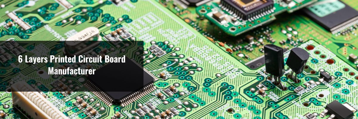
6 Layers Printed Circuit Board Manufacturer
Over the years, multilayer PCBs have gained immense popularity across industries. Today, it is easy to find several types of multilayer PCBs, including 4-layer PCBs, 6 layer PCBs, and so on. 6 layers PCBs have become an integral part of compact-sized wearable devices, as well as other mission-critical communication equipment. What makes them popular? How are they different from other types of multilayer PCBs? The post aims to answer everything that you would like to know about 6 layers PCB manufacturer.
An Introduction to a 6 Layers PCB
As the name suggests, a 6 layers PCB comprises six layers of conductive material. It is basically a 4-layer PCB with two additional signal layers placed between the planes. A typical 6 layer PCB stack-up features the following six layers: two internal layers, two external layers, and two internal planes— one for the power and other for the ground. This design improves EMI, and offers better routing for low and high-speed signals. The two surface layers help route low-speed signals, while the two internal buried layers help route high-speed signals.
|
Top Layer |
|
Prepeg |
|
Internal Ground Plane |
|
Core |
|
Internal Routing Layer |
|
Prepeg |
|
Internal Routing Layer |
|
Core |
|
Internal Power Plane |
|
Prepeg |
|
Bottom Layer |
The above shown is a typical design for 6 layer PCB; however, it may not be suitable for all applications. The next section concentrates on some probable configurations for 6 layer PCBs.
Key Considerations to be Made When Designing 6 Layer PCB Stack-ups for Different Applications
The right stack-up of a 6 layers PCB manufacturer will help you achieve a better performance, as it will help suppress EMI, use various types of RF devices, as well as include several fine-pitch components. Any mistake in the stack-up design will severely affect the PCB performance. Where to begin with? Here is how you can proceed with the right choice of stack-up.
-
As a first step towards the stack-up design, it is important to analyze and address the number of ground, power, and signal planes that your PCB may require.
-
The ground planes are an important part of any stack-up because they provide better shielding to your PCB. Also, they minimize the need for any external shielding cans.
The following are a few proven 6 layer PCB stack-up designs for various applications:
-
For denser boards with a small footprint: If you are planning to route a denser board with a small footprint, you can settle for four signal planes, as well as one ground and one power plane.
-
For denser boards that will use a mix of wireless/analog signals: In this type of board, you can opt for a stack-up that looks this: signal layer/ground/power plane/ground/ signal layer/ground plane. In this type of stack-up, the internal and external signal layers are separated by two ground planes that are encased. This stack-up design helps inhibit the EMI from mixing with the internal signal layers. The stack design is also ideal for RF devices, because the alternating power and ground planes offer excellent decoupling.
-
For printed circuits with sensitive traces: If you wish to build printed circuit boards with a lot of sensitive traces, it is better to settle for a stack-up that will look like this: signal layer/power layer/2 signal layers/ground/signal layers. The stack will provide excellent protection to sensitive traces. The stack is suited for circuits that utilize high-frequency analog signals or high-speed digital signals. These signals will be shielded from the low-speed signals on the outer layer. This shielding is done by the interior layer, which also allows routing signals with different frequencies or different switching speeds.
-
For boards that will be deployed near a source of strong radiation: For the boards of this type, the stack-up of the type ground/signal layer/power/ground/signal layer/ground will be perfect. This stack-up can suppress EMI efficiently. This stack-up is also suited for circuit boards that will be used in a noisy environment.
Benefits of Using 6 Layer PCBs
Six-layer PCBs are becoming a regular feature in several advanced electronic circuits, owing to their designs. The following advantages offered by these circuit boards have made them popular among electronic manufacturers.
-
Small Footprint: Owing to their multi-layered design, these printed circuit boards are smaller than other circuit boards. This is especially beneficial for miniature devices.
-
Quality-driven Designs: As discussed before, a 6 layer PCB stack-up design demands lots of planning. This helps reduce errors in their detailing, thereby ensuring high-quality construction. Additionally, nowadays all major PCB manufacturers are employing diverse testing and inspection techniques to ensure the appropriateness of these circuit boards.
-
Lightweight Construction: Compact PCBs are being materialized with the use of lightweight components, which help reduce the overall weight of a PCB. Unlike single or double-layered PCBs, the 6-layer circuit boards don’t require multiple connectors to interlink components.
-
Improved Durability: As depicted in the diagram above, these PCBs use multiple insulation layers between circuits, and these layers are bonded using protective materials, and different prepreg bonding agents. This helps improve the durability of these PCBs.
-
Excellent Electrical Properties: These printed circuit boards possess excellent electrical properties, which assures high speed as well as high capacity in compact designs.
It doesn’t matter, whether you are an established OEM or a novice electronic manufacturer, you will require high-quality 6 layers PCB manufacturer for your applications. Knowing their significance in your devices, it is important to source them from a trusted source such as Twisted Traces. The company has been providing quality-driven 6-layer printed circuit boards and multi-layer printed circuit board to its clients from past many years. Over the years, the company has designed circuit boards for use in miniature smart devices, military, and healthcare equipment.
.png)
