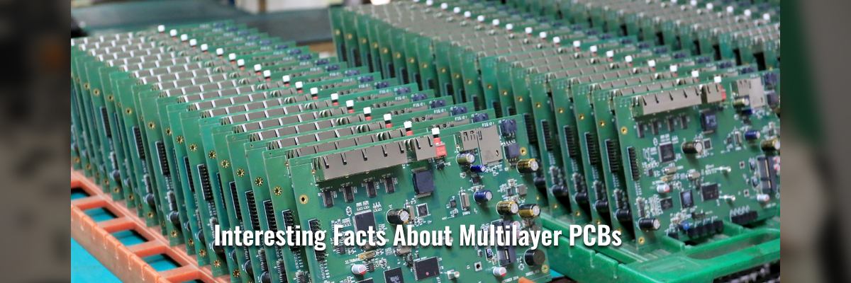

The development and implementation of multilayered PCBs is driven by necessity and increasing demand for miniature devices. Although PCBs have been used since decades in electronic devices; most of them were single or double layered with drawbacks such as noise and capacitance. Also, with the increasingly complex and miniature devices being designed and in demand nowadays, PCBs have also become smaller and layered to be fitted in any size and shape. Hence, multilayered PCBs were developed. Normally you can find four to 10 layered PCBs in many electronic gadgets such as smartphones. But the number of layers can go up to even 100 in certain complex devices and advanced circuits; however, this is not a very common feature. This post discusses some of the factors one should consider when deciding on the number of layers of PCBs and the benefits of multilayered PCBs.
Single layer PCBs are still used in simple devices. This comprises only a single layer of conductive material. Two-layer and three-layer PCBs are just as common. While these PCBs obviously have two and three layers, they also offer a better surface area much larger than that of a single-layer PCB. However, a multilayer PCB has to have at least three layers of conductor material. These materials can range from ceramic, glass, and aluminum to Teflon and FR4, usually with a copper foil. A multi-layer PCB manufacturer usually has a combination of single-sided and double-sided rigid PCBs. They are made of alternately arranged layers of prepreg and core materials. These are laminated air tight under high pressure and temperature. A melted and cured adhesive or a thin coating of it surrounds these layers for protection against the external environment and probable damages.
There is not much difference between prepreg and core materials except that core is cured, while prepreg materials are malleable and can be easily formed into sheets. When these materials are exposed to high temperatures, they melt and thus the layers are fused. They solidify once cooled.
Here is a representation of a multilayer PCB:
| Copper foil |
| Prepreg materials |
| Copper foil |
| Core materials |
| Copper foil |
| Prepreg materials |
| Copper foil |
There are many benefits of using multilayered PCBs for specific applications. Here are some of them:
As mentioned, multilayer PCBs are especially useful for small and high-end devices. They find applications in the following areas:
Are you looking for end-to-end PCB solutions for your applications? In case you manufacture electronic or electromechanical devices, you would require multi-layer PCB manufacturer . Ensure you approach reliable multi-layer PCB manufacturers for the same. Twisted Traces is a well-known manufacturer and assembler of various types of PCBs, which are RoHS compliant. They have a market presence of over 30 years.
.png)