
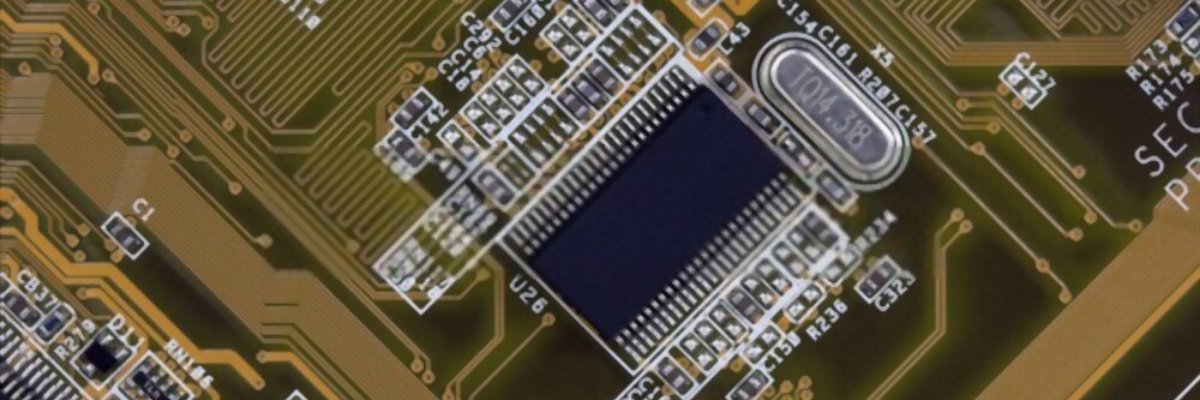
Inspection is an essential part of any manufacturing process, but it is especially critical when it comes to electronics and PCBs. The reason that inspection is important is because small mistakes during the fabrication process could render your entire product unusable. The quality of a PCB is determined by the quality of its components. These include solder mask, silkscreen, and substrate material, among several others. It is crucial to inspect these materials for defects before they are used in the manufacturing process. Inspections can be done manually or with automated production line equipment. The choice of equipment depends on the size and complexity of the boards being made. There are a number of different types of inspections used in the PCB manufacturing industry today, here we discuss one of the most prominently used technique, automated optical inspection.
Automated Optical Inspection (AOI) is a quality control technique used to analyze the surface of printed circuit boards. It is used to inspect parts after they have been manufactured to determine whether they are safe for further use. It is a testing method that scans the electronic board for possible defects, and it is conducted before or after the board has been assembled. This method automatically inspects the boards and detects minor defects without having to look at each solder joint individually. Its main uses include providing a high-speed and high-precision analysis of PCBs, increasing the speed at which PCBs can be inspected and reducing the number of human errors that occur during the fabrication process.
If you aren’t familiar with PCBs automated optical inspection, you should know that it uses a camera to check every layer of the PCB. The camera takes several pictures of each layer and then analyzes them against a database of acceptable results. It should be noted that not all automated optical inspection systems are created equal. There are many different models of AOI systems available in the market today, with different capabilities and performance levels. Some systems offer greater accuracy, while others have faster throughput speeds.
The AOI has many advantages over the manual inspection process. Some of the benefits of automated optical inspection systems are:
Needless to say, owing to the massive increase in the use of PCB, it is imperative to inspect them for any defects before shipping to the customer. This can be done manually with the help of human inspectors, but this process is highly time-consuming, expensive and has a high rate of failure. To solve this problem, automated systems has been introduced that not only reduce the manual effort and cost, but also ensure high accuracy in inspecting PCBs.
There are a large numbers of PCB manufacturers in the world, but not many can produce high-quality PCBs. It is not enough to just produce high-quality PCBs; it is also important to inspect every board to ensure their quality. Otherwise, you will end up with using low-quality PCBs that are not fit for use. This post ends by letting you know about a leading PCB manufacturer, Twisted Traces that uses automated optical inspection and ther inspection techniques to check defect-free boards.
.png)
