A Brief Discussion on Surface Mount Assembly Printed Circuit Board Process
A Brief Discussion on Surface Mount Assembly Printed Circuit Board Process
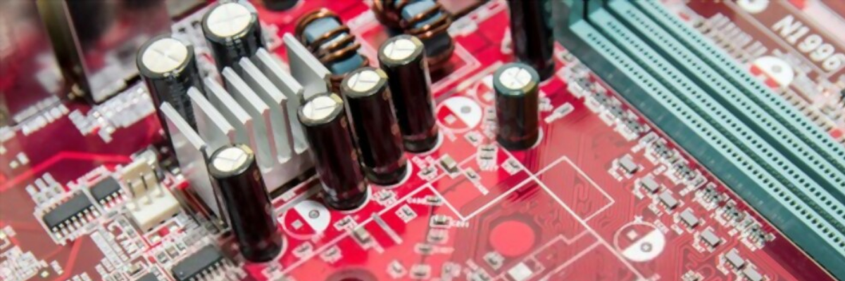
Printed circuit boards have been used in electronic devices since the 1960s. Today, they are an integral part of these devices, and contribute to their functioning and performance. If seen closely, these printed circuit boards bear several minute components, which are mounted on them perfectly. The underlying technology is referred to as surface mounted technology or SMT. Today, almost all PCB assemblies use several surface mounting components, owing to the advantages offered by them. Like any other PCB assembly process, the surface mount PCB assembly process also proceeds through different steps. This post gives you a brief outline of surface mount components and different processes involved in the SMT PCB assembly process.
Know About Different Surface Mount Component (SMC) Packages
As the demand for smaller and powerful devices are on the rise, so the importance of small surface mount component packages is growing. The SMC package appears like a flat structure with tiny lead pins soldered to them. However, they may differ in their structure. The following are a few popular types of SMC packages:
-
BGA: This is the abbreviation for ball grid array, which is the most popular surface mount component package. These packages are used for permanent mounting in devices like microprocessors.
-
SOIC: It stands for a small outline integrated circuit, which is thinner than DIP packages, and occupies less space than the latter. SOIC packages have contributed to the rise of thin small outline package (TSOP) and thin-shrink small outline packages (TSSOP).
-
QFN: It is an abbreviation of quad-flat no leads (QFN) package, which is a type of flat no-lead package. This package is similar to BGA, as well as QFP and helps connect ICs to the PCB surfaces effectively.
-
QFP: These surface mount component packages are easily distinguishable with their gull wing leads. QFP stands for quad flat package. It is available in ranges from 32 pins to 304 pins and pitch sizes from 0.4 to 1.0mm.
-
PLCC: Featuring a plastic casing, this surface mount component package shares close similarity with QFP, but has large pitch sizes than the earlier. This packaging is commonly used in programmable components, as well as NOR flash memories.
-
POP: An integrated circuit packaging method that is used to combine BGA packages and discrete logic packages to achieve higher component densities. This type of packaging is commonly seen in personal digital assistants (PDA), digital cameras, mobile phones, and so on.
An Overview of Surface Mount Assembly PCB Assembly Process
The surface mount assembly PCB assembly process starts with the selection of the components and creating PCB layouts using various software packages. The components for the PCB assembly are packaged in different ways such as tubes, reels, and trays. After these preliminary steps, the SMT PCB assembly process proceeds through the following steps:
-
Solder Paste Printing: The actual PCB assembly process begins here. Solder paste is applied to the PCB pad using a solder paste printer. The printer uses a stencil and squeezes the appropriate amount on the pad. This step forms the basis of PCB assembly, so, if anything goes wrong here, more defects will follow.
-
Inspection of Solder Paste: The solder paste inspection is performed using a built-in solder paste inspection system or a separate inspection system. This inspection allows PCB designers to check solder paste volume on the pad and print area, and so on.
-
Placement of Components: This step follows after PCB printing. All components are picked directly from their packaging using a gripper or vacuum nozzle, checked for appropriateness, and placed on the printed area at a high speed.
-
Inspection: Although the pick and placement machines are automated, it is important to inspect component placement before proceeding to reflow soldering. AOI machines are used for inspection of placement. They help identify the component presence, positioning, polarities, and value.
-
Reflow Soldering: This step follows the inspection of components. Electrical solder connections are made by heating the assembly to a pre-set temperature. Upon accomplishing all the above steps, reflow soldering may seem as a simple step. However, this is one of the most challenging steps because achieving the correct reflow profile is important. Any increase or decrease in temperature may damage solder joints.
-
Reflow Soldering Inspection: AOI inspection is conducted to check the quality of soldered joints. Along with this, X-ray inspection is also performed to check BGA component packages, voids or broken solder joints, and so on.
Owing to so many different technicalities involved, it is important that you partner with a trusted and experienced surface mount PCB assembly service provider like Twisted Traces. The company has been delivering customized surface mount PCB assemblies to its clients across industries.

.png)
