Printed Circuit Boards Layers Explained
Printed Circuit Boards Layers Explained
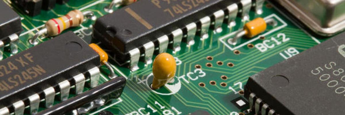
Over the years, printed circuit boards (PCBs) have undergone much experimentation and subsequent improvement, and advancement in their features. PCBs can have a single layer or multiple layers varying from 1 to 20 depending upon the design complexities and application requirements. However, there are two common layers on any PCB type. Would you like to know what are they?
What Are the Layers of Printed Circuit Boards?
The following list covers the most important part of the PCB layers. Multilayer PCBs primarily comprise internal and external layers. Here are the details.
-
Internal Layers: The internal layer sometimes called an inner layer in multilayer PCBs. Besides outer layers, these PCBs have several copper layers in between the top and bottom layers. These copper layers are called as internal layers. Sometimes, inner layers utilize the copper pour technique to create a power plane or ground plane. This technique reduces the amount of etchant used in the manufacturing process and also helps in the layer-to-layer bonding process. The weight and thickness of copper are customized based on the requirements of the application. The copper weight in the layer defines the minimum space and width that can be manufactured.
-
External Layers: External layers are often called as outer copper layers of the PCB. Several electronics components such as resistors, transistors, LEDs, capacitors, diodes, and more are attached to the external layers either by surface mounting technique (SMT) or soldering them into through holes. The external layer contains a copper foil, which is then electroplated with copper. This helps increase the thickness and add copper to the through-hole barrels. The finished copper thickness is customizable based on the requirement of the applications.
A Brief on the Number of PCB Layers
Nowadays, most PCBs are multilayered, thanks to the increasing complexities and shrinking sizes of electronic devices. The number of PCB layers largely depends upon your budget and application requirements. Also, considering the speed and frequency of the operation of your machine or device is key to deciding the number of PCB layers. Simple devices may do away with one or two PCB layers, and this reduces the unnecessary complexity as well as cost. For instance, coffee making machines, alarm clocks, and calculators of some examples of simple devices that can function with a single layer PCB. Examples of double-layer PCBs include HVAC systems, printers, and amplifiers. Multilayer PCBs comprise four layers and above and are fitted in more complex devices and machines in industries, smartphones and other handheld devices, and even some of the most complex equipment such as satellite systems.
More on Inner Layers
When it comes to inner layers, each layer has distinct features and functions. Some or all of these layers may be used in a PCB depending upon the design. Here are the details:
-
Mechanical layer: There may be one or several mechanical layers in a PCB depending on the design. There should be at least one mechanical layer as it outlines the physical dimensions of the board.
-
Solder paste layer: This is a material applied onto the PCB layers where components are mounted, mostly through soldering. It helps with the bonding of the solder with the component pin and improves the solder flow.
-
Solder mask layer: This layer is a mask or a protective coating applied onto the board to prevent damage and contamination. It is typically green in color; however, you can choose other colors such as blue and white depending upon your requirements.
-
Ground planes and power planes: These are copper layers, wherein the ground and the power planes are connected to an onboard voltage point.
-
Split planes: This is a modified version of power and ground planes, wherein they are split in a manner that they can be connected to multiple voltage points or potentials.
-
Keep out layer: This layer is crucial as it defines the working boundary and keeps it separate from the outer mechanical layer.
-
Silkscreen layer: This is typically the text displayed on the boards through which you can identify components with their names.
-
Routing layer: These layers help to interconnect the components. They can also be present on the top and bottom layers of the board.
PCB can be a single layer, double layer, or multilayer, but once you completely understand the purpose of each layer, then understanding the construction of PCB becomes easy, no matter how complicated the board structure. If you’re looking for highly-efficient printed circuit boards make sure you partner with a known and experienced PCB manufacturer like Twisted Traces. With over the 30 years of PCB design and manufacturing experience, they offer superior-quality printed circuit boards at competitive prices. Be it low-medium or high-volume PCB manufacturing requirement, their skilled and experienced team is up for everything.

.png)
