
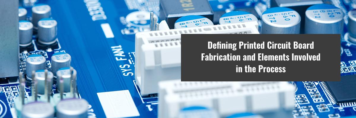
Printed circuit board fabrication can be defined as a process of putting together the layers of the board along with particular surface patterns before making it fully usable for electronics manufacturing. In a way, it is an assembly method that can be done either by the manufacturing firms themselves or by outsourcing the service to third party specializing in PCB fabrication.
The process of printed circuit board fabrication starts with a design or a diagram using client provided specifications and requirements. The PCB layout is an important part of the fabrication process. It involves a schematic design, which is created by the specialists after considering factors like: what the PCB is required to do, its functional attributes, and under what conditions would it be used. These details are provided by the customers or the clients to the PCB manufacturers who use the information for successful PCB fabrication.
The next step after understanding the definition of PCB fabrication would be to know what basic materials and methods go into the fabrication process of printed circuit boards. This information includes:
The Basic Board Materials
Ideally, the PCB base is made out of some non-conductive and solid material, which is then laminated with a copper sheet that creates the conductive surface. A type of glass-reinforced epoxy (known as FR-4) is most commonly used as a base material for general PCB design as the material is inexpensive, flame resistance and has low conductivity. For PCBs that are required for high performance, ceramic or PTFE bases with fillers are used.
Layers
Next, PCBs are made of layers of metallic sheets put together for high performance and efficiency factors. However, in case you require creating an inexpensive PCB for short term purposes, it can be fabricated with a single metallic layer. On one hand single layered PCBs are extremely easy to work with, but attaching electrical connections becomes inconvenient. Hence, most people prefer using and creating double-sided PCBs for ease of electrical connections and assembly.
Copper Traces
These are invariably the most important part of the printed circuit board fabrication process. It is important to pay complete attention to these thin fragments of copper intricately layered on the surface of the PCB. It is also crucial to consider the apt and exact size and thickness of these copper traces for the proper functioning of the PCBs.
Vias
These essential components are used in multi layered PCBs in the fabrication process as vias are required to electrically connect one layer to another. The 3 most common types of vias are-a) through-hole via, wherein a hole is drilled on the board, which is then electroplated for conductivity, b) a blind via is used to connect one layer with another without going all the way through, and c) buried vias are used only when it comes to connecting the internal layers of PCB fabrication.
It is important to understand that perfect and flawless printed circuit board fabrication depends a lot on the overall efficiency, performance, durability and functionality of the PCB and hence, it is critical to maintain certain levels of excellence while creating circuit boards for a particular application.
.png)