PCB Vias: Best Practices and Design Guidelines Discussed
PCB Vias: Best Practices and Design Guidelines Discussed
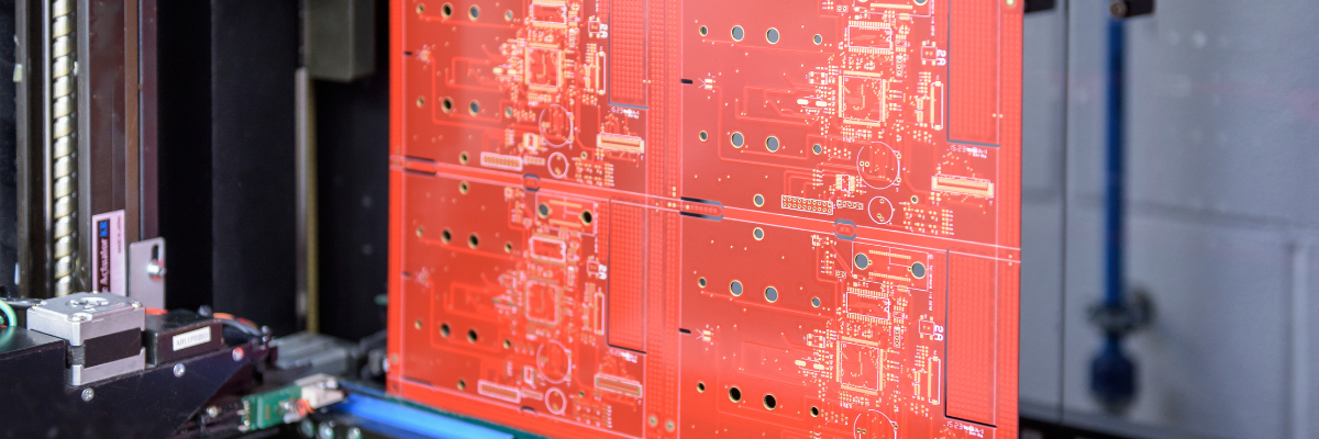
Printed circuit boards (PCBs) are the backbone of most electrical and electromechanical devices that allow the interconnection of components and facilitate the flow of signals. Designing these circuit boards is complex, demanding attention to detail and adherence to best practices. One critical aspect of the PCB designing process is the placement and optimization of vias. Vias establish strong electrical connections between PCB layers and allow seamless electrical signal flow. To ensure thermal management, signal integrity, and overall performance of PCBs, this post offers some PCB vias design guidelines that may be useful.
Essential PCB Vias Design Guidelines Every Designer Must Know
When it comes to PCB vias, following design guidelines can have a significant impact on the overall performance, manufacturability, and reliability of printed circuit boards. Consider the following key considerations to ensure optimal via design.
-
Via Types and Selection: This is one of the important PCB via design rules. Depending on the application requirement, choose the right PCB via type, such as through-hole vias, buried vias, blind vias, etc. If you aim to increase the routing density of circuit boards, choosing smaller-sized vias is recommended.
-
Strategic Via Placement: Vias should be placed strategically to improve signal integrity and minimize signal crosstalk. Ensure the proximity of vias to high-frequency components to minimize electromagnetic interference.
-
Via Size and Aspect Ratio: To ensure the manufacturability of your PCB, it is crucial to maintain an appropriate aspect ratio. Excessive aspect ratios can pose risks during the drilling process, leading to potential drilling issues and compromises in the overall quality of the board. When selecting PCB via sizes, it is important to consider the aspect ratio of the drilled hole in relation to the thickness of the board.
-
Clearance and Spacing: This is another important consideration while designing PCB vias for circuit boards. To ensure the integrity of your PCB design, it is essential to adhere to design rules and maintain adequate clearance and spacing between vias, traces, and components. Proper clearance and spacing contribute to reliable signal transmission, reduce crosstalk, and enhance your PCB's overall performance and functionality.
-
Thermal Management: To address heat-related concerns in the PCB design, it is recommended to incorporate thermal vias. These vias are strategically placed to facilitate effective heat dissipation and prevent overheating in areas with high-power components or significant heat generation. By allowing heat to escape efficiently, thermal vias help maintain optimal operating temperatures and prevent potential damage to sensitive components.
-
Signal Integrity: To preserve signal integrity in high-speed designs, adhering to impedance control guidelines is crucial. These guidelines ensure consistent impedance control across traces connected by vias, minimizing the risk of signal degradation and reflections. This ensures that the quality and reliability of the transmitted signals are upheld.
-
Design for Manufacturability (DFM): Performing DFM is crucial in the PCB via design. These checks involve analyzing the design for potential manufacturing issues related to vias. By conducting DFM checks, you can proactively identify and address issues early in the design process, saving time and avoiding costly manufacturing errors. Collaborating with the PCB manufacturer can streamline the manufacturing process and ensure that the via design meets all the necessary manufacturing requirements.
-
Verification and Testing: To ensure the functionality and performance of vias in your PCB design, it is essential to conduct thorough design rule checks (DRC) and simulations. DRC checks verify that your vias meet design specifications and guidelines, including clearance, spacing, and other critical parameters. By performing DRC, you can identify and rectify any design issues before fabrication, thus reducing the risk of manufacturing errors later.
By now, you have got an idea about PCB vias design guidelines. These guidelines are crucial in improving board density and reducing production costs. With advancements in high-density designs, manufacturing circuit boards has become easier. However, it is important to ensure accurate requirement sharing to obtain the appropriate PCB vias for your design. In case you have any questions on this PCB vias design, consulting a trusted industry player like Twisted Traces is highly recommended. With their extensive market experience and a team of experts, the company utilizes reliable via filling processes to design and manufacture circuit boards.
.png)

