PCB Testing and Inspection Helps Improve its Reliability
PCB Testing and Inspection Helps Improve its Reliability
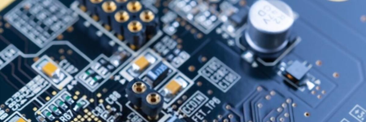
As known, PCBs are integral components of all electronic devices, which is why they are subjected to rigorous inspection and testing at every phase of manufacturing. Several techniques are employed by manufacturers and assembly services to assure the reliability of printed circuit boards. Although there has been quite a lot of literature available on testing and inspection techniques, there is no information available on factors or criteria for reliability testing.
A Brief Outline of Popular PCB Testing and Inspection Techniques
Before going into details of reliability testing of PCBs, lets focus on some of the popular PCB testing and inspection techniques employed by PCB manufacturers. As their reference would give clarity to type of defects detected by using them.
-
In-circuit Testing: This is one of the popular testing techniques adopted by PCB manufacturers owing to 98% capability that it assures. ICT features software, an in-circuit tester, and a fixture that can detect most defects during the manufacturing process.
-
Bed of Nails Texture: This testing uses multiple pins, especially pogo pins, to establish contact with different test points on the PCB.
-
Flying Probe Testing: This is another popular technique, which uses small pitches to establish the contact with SMD pins and other test points. Flying probe testing is more suited for small contacts.
-
Automated Optical Inspection (AOI): As the name suggests, this PCB inspection technique uses cameras to check the PCBs for defects. The software in the automated machine compares the PCB to be tested with a reference board.
-
Automated X-ray Inspection (AXI): This technique utilizes X-ray to detect defects that are not visible to human eyes. AXI is employed to identify defects under the IC packages such as Micro BGAs, BGAs, CSPs, LGAs, and so on.
Factors Checked to Ensure Reliability of PCBs
Having known the popular PCB testing and inspection techniques, you may be interested to know the defects detected by them, isn’t it? The following list offer insights on the type of defects identified during the reliability testing.
-
Copper Plating: copper is laminated on the board to improve its conductivity. During PCB testing and inspection, copper plating is subjected to tensile strength and elongation test.
-
Lamination: Quality of lamination plays a key role in the performance of the PCB. At times, it may peel off due to application of heat or force.
-
Electrical Conductivity: PCBs are tested to ensure they pass the entire current with minimal or no leak.
-
Environment: In most industrial applications, PCBs are subjected to moisture or heat. The PCB is tested for moisture absorption and humidity. PCBs are weighed before and after the moisture and humidity test and any changes in weight is considered as a defect.
-
Hole Wall Quality: PCB holes may delaminate or crack under heat, which is tested during the PCB testing and inspection. The holes are tested for thermal stress and shock absorption qualities.
-
Solderability: During PCB assembly and manufacturing components are soldered to the board in soldering oven or using advanced equipment. Soldering defects such as opens, shorts, excess or insufficient soldering, and voiding can affect the performance of the PCB. So, these defects are identified during AXI. However, that is not enough. As a part of reliability testing, the PCB is subjected to wetting test. The term wetting refers to the ability of the surface to accept the liquid solder.
If you are planning to invest in quality PCBs, it is always important that you source them from experienced manufacturers, with specific experience in serving clients from your industry. Twisted Traces is one of the experienced manufacturers of industrial PCBs in the US. The company has been providing quality-driven PCBs in various dimensions to its clients across industries. The experts at the company employ various advanced and proven testing and inspection procedures to conduct reliability testing and to check and rectify the defects before the PCBs are shipped out of the facility.
.png)

