PCB Fabrication Calculator
PCB Fabrication Calculator
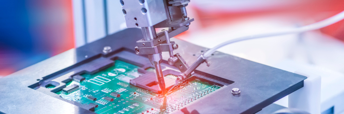
Printed circuit board fabrication is a broad term that encompasses various processes and components needed to build a working circuit board. These circuit boards are the basic building blocks of all modern electronic devices. The layers on the circuit board are organized in a specific pattern to meet application requirements. Most businesses either manufacture circuit boards in-house or they outsource it to third-party providers such as Twisted Traces. How much does a PCB fabrication cost? This is one obvious question asked by electronic OEMs approaching Twisted Traces. To simplify the things, the PCB fabrication cost calculator is provided on the website. How does the PCB fabrication cost calculator work? What are its typical features?
Features of PCB Fabrication Cost Calculator
Twisted Traces provides high-quality printed circuit boards at consistent prices. We can create a single board prototypes or produce them in large quantities depending on the customer requirements. As any fabrication process, the PCB fabrication process is an intricate process and it involves several features. The following are important features of a PCB fabrication cost calculator. Your responses will help us provide you an appropriate PCB online quote.
-
PCB Part Number: Here you have to enter your PCB part number. This is not a cost-incurring field, yet it will help us understand your requirement better.
-
Board Type: We allow users to select from three options – Single Pieces, Panel by Customer Design, and Panel by Twisted Traces. This means we can provide you a single board or the panel can be arrayed with several PCBs of the same type or different type. If you do not make the right selection, we will consider it as Single Pieces (set as a default).
-
Layers: This is the most important field in the calculator and one of the most important cost-incurring factor of the PCB fabrication. Here basically you have to select the number of copper layers in the PCB. We provide PCBs in – 1-2 layers, 4 layers, 6 layers, and 8 layers. The calculator provides you cost for 1-2 layers and 4 layers. Please request a quote for 6 layers and 8 layers.
-
Board: This is the desired dimension of your board. Here you have to enter board width (X) and board length (Y) in inches or millimeters.
-
Under board width (X), enter any value from 0.5 to 11mm for 2 layers PCB, and 0.5 to 0.9mm for 4 layers, 6 layers, and 8 layers PCB
-
Under board length (Y), enter any value from 0.5 to 17mm for 2 layers PCB and 0.5 to 15 mm for 4 layers, 6 layers, and 8 layers PCB
-
This attribute is invisible for the Panel by Customer Design option.
-
Quantity: This refers to the number of boards required in order. You can enter any value between 1 and 100 pieces. You have to request a quote for pieces from 101 up to 50,000. The quantity is invisible for the Panel by Customer Design option.
-
Different Design in Panel: This refers to the number of PCBs in a panel. You can request multiple PCBs at the same time. In this case, we may organize the different PCBs on a single panel. They can choose from 1, 2, 3, 4, 5, and more than 5 designs on a single panel. We charge extra for populating different designs on a single panel, where there are no extra charges for the same PCB design arranged on a single panel. If you do not select any value, then we will consider it as 1 design on a single panel.
-
Material: This refers to the base material for the PCB. It is set at FR4 TD350 (TG180) by default. Do you have any other requirement? Please contact us at the earliest.
-
Board Thickness: This refers to the desired thickness of the printed circuit board. You can choose from five given options - 0.031", 0.062", 0.093", and 0.125".
-
Outer Layer Copper Weight (Finished): The thickness of copper is an important attribute for any PCB. It contributes to the current carrying capabilities of a PCB. Copper weight refers to the weight of copper in one square feet of PCB. You can choose from 1 Oz to 2 Oz for your outer layer. 1 Oz is the default value for this attribute.
-
Inner Layer Copper Weight (Finished): This is the thickness of copper within the PCB. You can choose from values 0.5 Oz, 1.0 Oz, and 2 Oz copper weights.
-
Surface Finish: The surface finish helps concede the copper layer and improve its solderability. We offer various types of PCB surface finishes to meet the diverse complex needs of our customers. They can choose from the following options:
-
Hot Air Solder Level (HASL) Leaded: It is a tin lead solder coating. This surface finish is one of the most popular on this list, and it assures excellent shelf life than other surface finishes. The surface finish is thickly coated over the board. This thick application reduces the planarity of the board, which is not desirable for fine pitch components. This finish also improves the re-workability of the board.
-
HASL Lead Free: This is a lead-free and ROHS-compliant version of HASL leaded surface finish.
-
Electroless Nickel/ Immersion Gold (ENIG): This surface finish features nickel and gold. Nickel acts as a copper barrier, and components adhere on it. Gold helps secure nickel during the storage. This surface finish assures a planar surface, long shelf life, and is ideal for PCBs comprising plated through-hole components. ENIG has an RoHS-compliant surface finish, and can resist handling, as well as environmental conditions.
-
Immersion Silver: The surface finish helps produce strong solder joints, and also assures a planar surface. This RoHS-compliant surface finish features a thin silver lining made over the copper trace. It is not recommended for applications, where the boards may be exposed to humidity, moisture, or other environmental conditions. Also, it cannot withstand rough handling. It is ideal for single pieces and large volume pieces. It helps reduce frequency loss due to skin effect.
-
Minimum Tracing/Spacing: This is the smallest distance between the two conductors that are placed adjacent to each other. It is perhaps the smallest width of the conductor. You can select from two values – 5/5 mil and 6/6 mil.
-
Minimum Hole Size: This is the smallest size of the hole. You can select from two values – 10 mil and 12 mil.
-
Solder Mask Sides: Solder mask creates a barrier between the conductors and soldered joints on the PCB. They help prevent the formation of solder bridges and oxidation of copper traces that serve as conductors. You can choose from – None, Top, Bottom, and Both.
-
Solder Mask Color: This refers to the color of protective coating or soldermask to be applied to the PCB. You can choose from colors – Green, Red, Blue, Black, and White. This feature remains hidden, if you choose “None” in the earlier field - Solder Mask Sides.
-
Silkscreen Sides: It is the text-based information printed on the PCB, which may indicate company logos, components reference, component identifiers, and so on. The silkscreen is used to identify different types of components, as well as soldering. You can choose to apply silkscreen on top and bottom. The calculator provides you options – None, Top, Bottom, and Both.
-
Silkscreen Color: The information can be printed in various colors. You can choose from the options – White, Black, Yellow & Red. This option remains hidden if you choose Silkscreen Sides as None.
-
Full Design Rule Check: This is one of the major steps involved in the physical verification signoff on the design. Full design rule check involves Layout versus Schematic (LVS) check, XOR checks, Electric Rule Checks (ERC) and antenna checks. You can choose Yes or No from the calculator.
-
Impedance Control: Impedance is the resistance to the flow of current. In high-frequency circuits, it is represented by an electrical network of combined capacitance, resistance, and inductance reaction. You can choose from Yes or No options.
-
Blind and Buried Via Present: A blind via is used to connect the outer layer to one of the inner layers, and it doesn’t propagate through the entire board. A buried via connects different inner layers, it doesn’t touch the outer layer. These vias add to the cost of the PCB. If you choose Yes from the calculator, then you need to request a quote. Our team will understand your requirements before providing you the quote.
-
PCB Fabrication Lead Time: This is the time taken to manufacture a PCB. We can provide these PCBs in 2 days, 3 days and 5 days depending on your requirement.
-
Detailed Information/Special Requirement: Do you have any specific requirement that is not covered by the calculator? If yes, you can enter your requirement in the box provided. This will help us understand your requirements, and provide you an appropriate service.
The PCB fabrication calculator is designed such that it eases all doubts that you may have in mind when it comes to understanding the costs associated with PCB fabrication. For gaining an in-depth understanding of various factors mentioned in the calculator, you can always get in touch the team at Twisted Traces.