
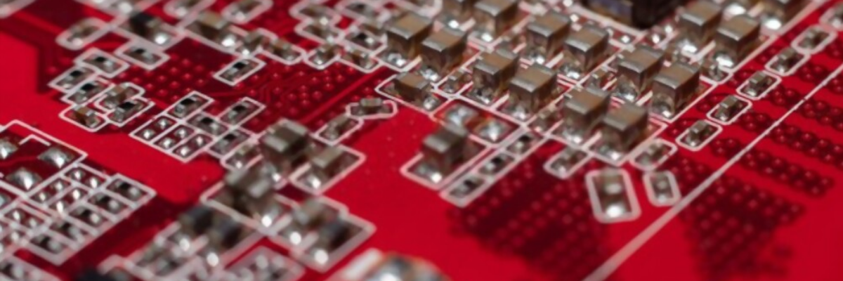
Printed circuit boards (PCBs) being the core of most digital as well as electromechanical devices must be perfect in terms of design, functioning, and so on. Their accuracy directly impacts the functioning and enhancement of the product. So, it is crucial that PCB design is flawless and there are stringent testing and inspection techniques implemented at all stages through the manufacturing process. There are many types of testing techniques such as manual, automated optical inspection, X-ray inspection, and so on performed at specific stages. X-ray inspection is one of those widely used testing techniques for PCBs and assemblies to find out hidden defects and enhance quality.
PCBs find applications in crucial sectors such as defense, medical, aerospace, heavy engineering, automobile, and so on. Such PCBs often undergo x-ray automated inspection. As the term implies, x-rays are used to identify hidden manufacturing defects in a circuit board. This is because x-rays can penetrate through the components, joints, wiring, and solders, and scan the board in detail. This makes it easy to identify hidden issues which may not be otherwise noticed. Also, with the growing demand for component dense and complex yet small-sized boards, this inspection type becomes essential as it may be difficult with only visual inspection as well as thermal imaging to scan through such intricate wiring, closely placed components, hidden solders, open shorts, wrongly aligned wiring, and so on.
X-rays not only penetrate deep inside the components and solders but also get absorbed by them depending on the materials they are made of and their atomic number. The higher the atomic number the better the absorption of x-rays. This results in enhanced and clear images of the parts and components. Materials with low atomic weights let x-rays penetrate through them; however, this image is more like rays passing through transparent objects. The device used for x-ray inspection comprises the following components.
The x-ray tube is passed through the boards to be inspected. As mentioned, based on the atomic number of the materials, the rays go deeper. These are converted into images which are projected on the detector. These devices have additional features such as high levels of magnifications for close zoomed in views, oblique angle inspection for a detailed analysis of ball grid arrays, solder joints, CSPs, and so on. Some models have 3D imaging features. Both 2D and 3D viewing features are there in most devices, and most engineers prefer simultaneous viewing of an image in different angles. In 2D, you can view each component from all sides and different angles, while in 3D, 2D images can be rebuild for cross-sectional viewing. The x-ray tube may be closed or open and with different magnification levels, filament types, and voltages. Tubes with low voltages are fine for simple boards with few components or single-sided boards. High voltage x-ray tubes are needed dense and complex boards.
If you are an OEM who needs PCBs assembly for your product or application, ensure you partner with an experienced PCB manufacturer and service provider who is focused on quality. Also ensure, they perform stringent testing techniques on the PCBs and assemblies before installation. It is also important for the service provider to understand your requirements offer maximum customization for better fitment. Twisted Traces is a custom circuit board manufacturer offering end-end services for PCBs and assemblies.
.png)
