Know the Advancements in PCB Manufacturing Processes
Know the Advancements in PCB Manufacturing Processes
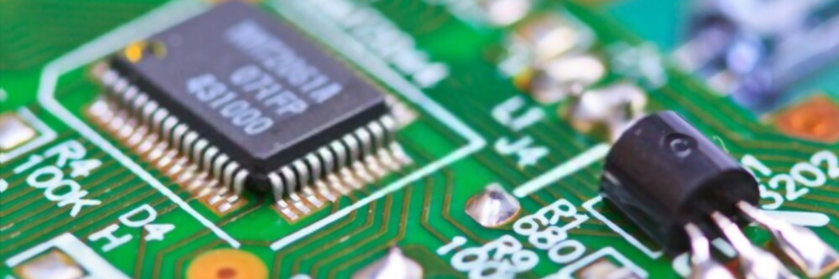
While PCBs have been in use from several decades, they have newfound applications in several industrial segments. This is primarily because electronics has found its way in nearly all the sectors including medical, defense, and many more crucial industries and has changed the way they function. PCBs and their manufacturing processes also have much evolved over the last three decades or so with advancements in CNC machines, fabrication processes, and a heavy demand for small circuit boards with several components. The PCB design should be such it manages high voltage, high power boards with multiple layers, and more. This post discusses the advancements and recent trends in PCB manufacturing processes.
Advanced PCBs and Manufacturing Processes
Advanced PCBs in general have some peculiar characteristics such as a very tight tolerance for solder mask offset, minimal trace width without fill lines, plugged vias, a very tight level of dimensional accuracy, and more. These are commonly used in electronics and telecommunication, instrumentation, biomedical, defense, industrial equipment, and more. Most of these advancements have evolved over the years with standard PCBs still being produced and used. Many advancements continue to be under research as PCB manufacturing processes, materials, components, and equipment must continually improve and evolve hand in hand.
Current trends in PCB Manufacturing Process
The phrase “Change is the only constant” can be very easily understood if we study the timeline or evolution of the PCBs and electronics sector, and their ever increasing applications. PCB requirements and subsequently their manufacturing processes have evolved over the years. Here, continuous improvement in devices which will lead the innovation in new generations of electronic products is the main goal. Hence, the advancement happens at the base or core which is the PCB level. Here are some related current trends.
-
Flex circuit boards: There is an evolving trend of using completely flexible boards rather than rigid or rigid-flex ones. This is mainly because of the bending angles and flexibility they offer. They can be made in small sizes while also accommodating several components and layers. Also, you get several options for materials which can withstand harsh environments.
-
Internet of Things (IoT): Device to device communication has picked up pace over the last few years, and this is only likely to increase over the next few years. Smart devices ranging from phones and electricity meters to refrigerators, lighting systems, and other home and industrial systems are all a part of IoT. The fact that these smart devices function on an auto mode, sense things, issue messages and alerts accordingly, and enable remote access, monitoring, and control, is attributed to their complex PCB design.
-
High power boards: These boards have supplies of up to 48 volts. These are commonly used in electric vehicles for which the demand is quite high and expected to increase further. However, to eliminate noise and interference issues, these boards need large components mounted on them, including a battery pack.
-
High density interconnects (HDIs): This is already much in use and has a huge demand as the size of digital devices continues to shrink. This technology facilitates compact boards with limited number of layers with high-speed signal transmission. This technology continues to be under research to overcome issues related to noise, fabricating traces in a small area, and so on.
-
Board Cameras: These are cameras directly mounted onto a PCB. They are small in size and hence can be easily fitted onto a board. They are capable of taking high definition pictures and videos quite easily. While they are much is use and demand, further research might yield better results which may help in improved industrial solutions and other applications.
-
Auto routers in PCBs: Modern PCBs have an auto placer or auto router in their design which facilitate automation by automatically routing digital functions throughout the board to determine the PCB layout features. This component speeds up the automation in a product. However, this also needs further research in terms of easing the installation and setup and also catering to specific product design requirements.
-
Biodegradable PCBs: Much is being discussed about using ecofriendly devices and products which can be recycled or reused. The same applies to PCBs as well as e-waste or electronic waste is a huge concern. As part of reducing the carbon footprint, researchers are developing biodegradable materials for PCBs, with some even suggesting changes in the manufacturing process. However, this needs more research and hopefully there may soon be a concrete solution to this issue.
If you are an OEM who has manufactured a partially or fully automated product, you may require a complex PCB design. Ensure you partner with a reliable PCB manufacturer and services provider who has several years of experience and used advanced PCB manufacturing processes. Twisted Traces designs, fabricates, and assembles various types of PCBs using the most advanced PCB manufacturing processes, materials, and fabrication techniques.

.png)
