Know How to Save on Your High-density Interconnect (HDI) PCBs
Know How to Save on Your High-density Interconnect (HDI) PCBs
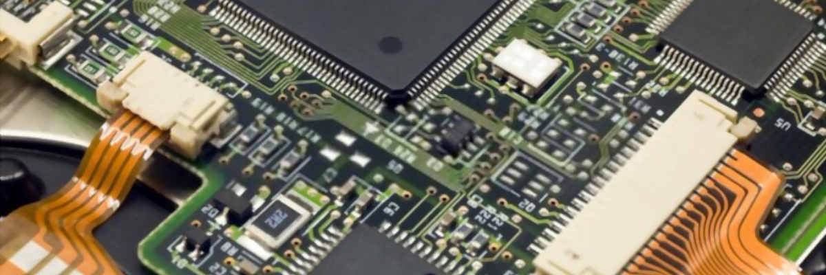
High-density interconnect (HDI) PCBs are the most in-demand printed circuit boards, which are widely used in various compact-sized, high-performance electronic devices. As the electronic devices and their components are getting smaller, these printed circuit boards pack more circuitry and functionality in small areas. They comprise microvias, buried and blind vias, and through-holes. In addition to this, the PCB may possess a coreless construction with layer pairs, passive substrate construction without an electrical connection, and connections with coreless builds and layer pairs. Although an HDI PCB looks compact, it involves detailing and several complex elements, which add to its costs. This post offers tips on how to reduce the costs of HDI PCBs without compromising on quality and performance.
A Brief Discussion on Few Factors That Add to the Cost of HDI PCBs
The cost of the HDI PCBs may be affected by several factors. Addressing these factors and choosing the right alternatives will help you save on PCB manufacturing costs and optimize the value of your PCB investments.
-
Choose the Type of Vias Properly: Via is a term for an electric connection made between two layers of the PCB. The vias feature two pads, which are positioned adjacent to each other on two different layers of the board. Blind vias are usually exposed to a single side of the board, while buried vias are not exposed on the board, but they connect the two layers internally. Microvias are small vias with a hole diameter of 0.15mm. They are usually drilled using laser equipment and demand high precision. It can be easily understood that microvias can add to your costs more than other via types. So, it is always wise to choose the type of via keeping the application requirements in mind.
-
Stackup Height and Number of Layers: The stackups are one of the prominent features that add to the cost of PCB assemblies. 1-n-1, 2-n-2, and 3-n-3 are the most common types of HDI stack-ups. A 2-n-2 layout is considered challenging than 1-n-1, and 3-n-3 is even more challenging than 2-n-2. This is because the efforts increase as the number of layers go on increasing.
-
Material Chosen: Fiberglass, FR4, and copper are a few popular core materials used for building HDI PCBs. These materials possess different physical properties, so their costs also differ. When choosing the material, it is important to focus on three properties – the dimensional stability of the material, machinability, and ability to withstand multiple laminations. The HDI design involves laser drilling and if the material cannot withstand drilling then it can be problematic. Hence, it is important to ensure the material meets all these requirements while offering a price advantage.
-
Stacked and Staggered Set Ups: The stacked vias are usually filled with copper, while staggered vias are not filled. No extra imaging step is required in the staggered vias. However, planarization as well as extra imaging step, are required in stacked vias. All these makes staggered vias pretty simple in comparison to stacked vias. The simplicity helps cut down the manufacturing costs further.
-
Conductive or Non-conductive Hole Fill: This is also one of the important pricing factors. The conductive or non-conductive hole fill process depends on the design. Some designs require vias below the surface mount component, which needs to filled, capped, or plated. The filling process usually requires multiple plating and drilling steps, which may demand additional time and effort.
Although focusing on the above factors will help you save on HDI PCB costs, you can save more by partnering with an experienced PCB manufacturer. Twisted Traces is one of the most popular and experienced PCB manufacturers in the US. The experts from the company work closely with clients to understand their requirements while offering them value-driven and cost-effective solutions.

.png)
