Key Information on Bare Board Printed Circuit Boards Covered
Key Information on Bare Board Printed Circuit Boards Covered
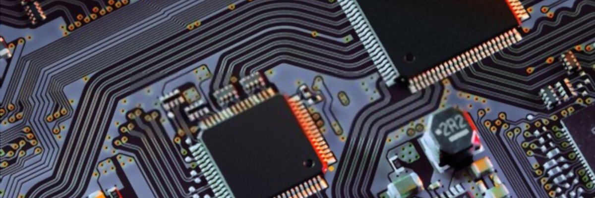
Bare boards play a key role in printed circuit board development. As the demand for dense and compact-sized electronic devices are increasing, the design and assembly requirements change regularly. The bare board printed circuit boards form the core of these electronics. Design engineers use these bare boards to lay the design of the circuit boards and populate components over them. Although the bare boards may look simple and easy to work upon, there are several things to be addressed while working with them. This post introduces you to bare board printed circuit boards and details you would like to know about them.
Important Things You Need to Know To About Bare Board Printed Circuit Boards
Bare boards are the simplest form of printed circuit boards you can think of. The following pointers will help you understand them better.
-
A bare board comprises three elements – conductive pathways, metal coating, and substrate.
-
As the name suggests, the conductive pathways, as well as patterns direct electricity through them.
-
The bare boards also perform another function – they support the pads, traces, conductive tracks, and so on.
-
The conductive traces are etched on these bare boards by etching. This etching is performed on copper sheets, which are then laminated on a substrate, which is a non-conductive material.
-
The process of mounting components on the bare board is known as PCB assembly.
-
Bare board printed circuit boards are generally made of materials like FR-4, FR-406, G10, FR-408, Rogers, CEM3, and Alumina.
-
The layout of components on the bare board is performed using software applications. Altium and CAD are two prominent software applications generally used for the purpose.
-
The bare board is tested to ensure the working of the PCB circuit. This testing enables to check the validity of key functions such as isolation between circuit patterns, and stability between pads that are interconnected to each other.
-
A bed of nails fixture is used to test the connectivity between pads.
-
Flying probe testers are used for testing and they feature multiple robotic arms with robes equipped to them, which easily glide across the surface.
-
Bare boards printed circuit boards that have not been tested are likely to fail when used directly in applications and it may lead to rework and product recalls.
-
By integrating the testing of bare boards from the beginning, one can easily streamline different aspects of production.
If you looking for high-quality bare board printed circuit board designing and fabrication, you must partner with a trusted and experienced manufacturer. Twisted Traces specializes in bare board printed circuit board manufacturing. The company provides single layer, double layer, and multi-layer rigid, rigid-flex, and flexible printed circuit boards in different configurations. The company has been successfully serving its clients across the military and defense, medical, software, consumer, and industrial electronics industries for several years now. The company specializes in customized printed circuit boards, so, you can get in touch with the team today to discuss your requirements.
.png)

