
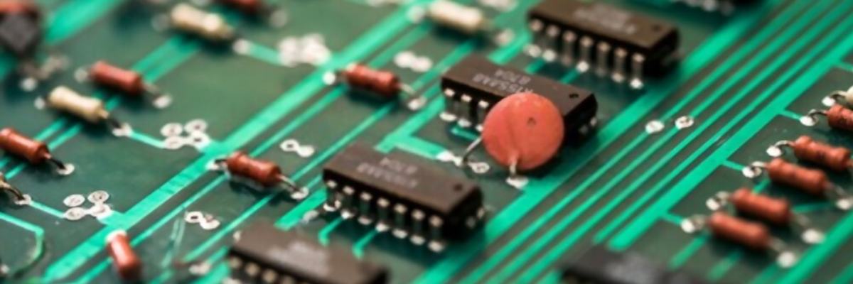
With increasing awareness about the side effects of leaded and halogen materials used in different electronic products, many world governments are imposing stringent laws and regulations to curb their use. As a result, the demand for environmentally-free electronic products has increased in recent years. Having said that, most of these products are driven by PCBs, built using halogen-free materials. Although in physical appearance, the halogen-free materials may look similar to regular PCB materials, their dissipation factor, dielectric constant, and moisture diffusivity largely differ. What are halogen-free PCBs? What are the popular applications of these PCBs? How they can add value to your application? Read this post to get answers to all questions that you may have regarding these PCBs.
Halogen elements are the Group 17 elements in the periodic table. Fluorine, chlorine, bromine, Atastatium, and iodine are the popular halogen elements known to us. These halogen elements are known for their fire retardant capabilities, which makes them an ideal choice for electronic applications where high temperatures may be involved. Most printed circuit boards that we use today are built using FR4 and CEM3 flame retardant materials, which feature halogens.
Many studies conducted across the world suggest that halogen-containing flame retardant materials are dangerous to human health and the environment. They emit toxic gases and release harmful byproducts into the air when burnt and both these can have severe consequences for humans. Bromine and chlorine exposure results in blurred vision, coughing, nausea, skin irritation, burning nose, eyes, and throat. Prolonged exposure to these halogens can be detrimental. As a result, the RoHS Directive published in July 2006 banned two most used halogenated flame retardants - polybrominated diphenyl ethers (PBDE) and polybrominated biphenyls (PBB). Other substances were added to this list in later years.
A halogen-free PCB is a type of PCB made of copper-clad laminates with bromine (Br) and chlorine (Cl) content less than 0.09% weight ratio, as defined in the IPC/JEDEC J-STD-709 standard.
The PCBs made of halogen-free compounds offer several benefits over regular PCBs, which accounts for their increasing popularity in many applications. The following are a few advantages of halogen-free PCBs.
The PCBs made from halogen-free compounds are widely used in the following applications:
Over the years, these printed circuit boards have become a common choice in power stations, substations, laboratories, distribution rooms, and so on. Halogen-free PCBs are expensive than conventional PCBs due to material designs, costs of materials, and complexities involved. Thus, you must source them from experienced manufacturers like Twisted Traces. The company provides leaded and RoHS-compliant and halogen-free PCBs for use in medical, consumer electronics, industrial electronics, municipal applications. All PCBs are entirely made in the company’s well-equipped facility at Elk Grove Village, Illinois and offer high-quality PCB fabrication.
.png)
