Best Practices for PCB Silkscreen Design
Best Practices for PCB Silkscreen Design
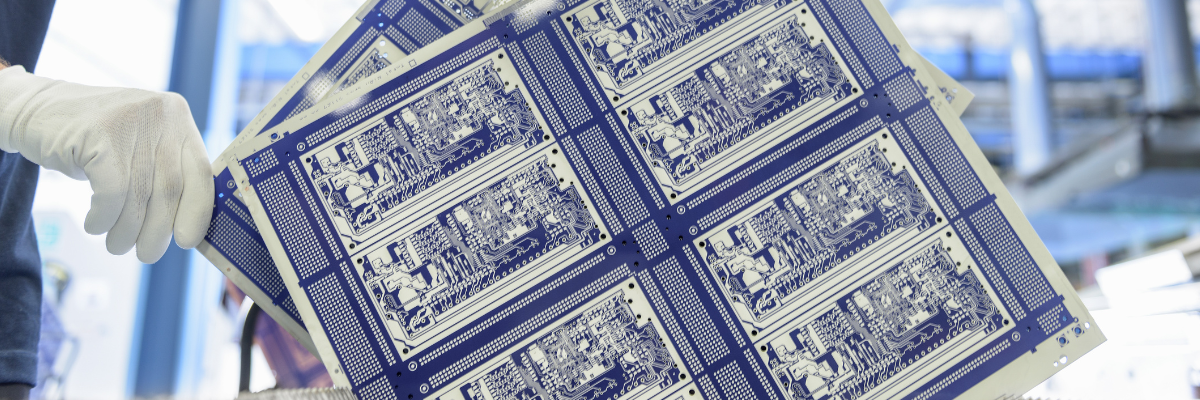
Designing printed circuit boards (PCBs) demands attention to detail to ensure error-free and performance-driven PCBAs and the final product. One of the important aspects of PCB design is the silkscreen layer. It is the layer of markings used to identify the PCB components, logos, and symbols on the board's surface. Silkscreen is valued for the information it delivers such as component placement, warning symbols, polarity of parts, manufacturer's mark, and so on. An effectively designed PCB silkscreen eases PCB assembly and debugging, enhances the user experience, and promotes brand identity. Considering the importance of PCB silkscreen, are you intrigued to know how to include PCB silkscreen in the design effectively? What key pointers to consider when designing PCB silkscreen? Read this post till the end.
Standard Guidelines for PCB Silkscreen Design
Here are some general guidelines for creating well-organized and effective PCB silkscreen designs.
-
Keep it Simple and Clear: PCB silkscreen conveys vital information to technicians, engineers, and end users. Thus, it should be designed in a simple and easy to understand manner. Also, the font should be readable and in appropriate sizes. Avoid overly elaborate fonts, which are difficult to decipher, especially when working with compact, multilayered PCBs.
-
Adequate Text Size and Spacing: Another important factor in silkscreen design is the size of the text. The text should be large enough to be read easily without magnification. A good thumb rule is to use a minimum of 1mm text height; however, this may vary based on the size and complexity of the circuit board. There should be enough space between silkscreen elements and components to prevent overlapping.
-
Use Conventional Component Names: Consistency is key in silkscreen design. It is important to use conventional component names and reference designators that are recognized in the industry. This helps technicians and engineers identify and understand the components during assembly and troubleshooting.
-
Differentiate Silkscreen from Solder Mask: It is essential to differentiate silkscreen and solder mask for manufacturability. Using contrasting colors for the solder mask and silkscreen helps prevent confusion during production. For instance, the most popular combination is a white silkscreen on a green solder mask.
-
Placement of Silkscreen Elements: The placement of silkscreen elements is crucial as it can significantly improve the overall design. Ensure the component names and reference designators are placed near their respective components without obscuring important markings or pads. It is always the best strategy to place a text horizontally whenever possible. Also, consider rotating it if there is a space constraint.
-
Avoid Silkscreen over Pads and Traces: Silkscreen elements should not overlap with other components to prevent potential issues during manufacturing, such as accidental short circuits or misalignment. There should be enough distance between silkscreen elements and copper features, especially in areas prone to soldering or rework.
-
Test for Clarity: Conducting a clarity test before coming to any final decision is essential. Print the PCB layout in the desired size and inspect it for readability. Take an expert’s feedback to ensure the silkscreen elements are clear and easily understandable.
-
Design for Multi-layer PCB: Take note of PCB layers when designing the silkscreen. In multilayer PCBs, components may be sandwiched between inner layers, making them inaccessible. Ensure a plan for additional silkscreen elements on the outer layers to aid component identification and assembly.
An effective silkscreen can enhance the overall circuit board design and manufacturing process. By adhering to the aforementioned practices, designers can assure that the silkscreen is visually appealing and informative. Considering the importance of PCB silkscreen, it is good to consult a trusted and experienced manufacturer like Twisted Traces. Their team of experts is experienced in offering all forms of silk screening considering the application requirement. If you feel stuck in selecting the appropriate silk screening, they will assist you in all possible ways. For any technical assistance or pricing-related questions, feel free to contact their team via phone or email.
.png)

