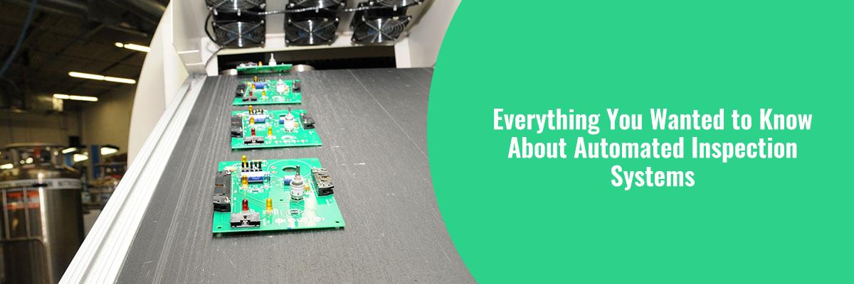
Automated Optical Inspection (AOI) is as the name suggests a visual quantitative and qualitative test for PCBs. This automatic process allows companies to reduce their dependency on manual testing and thereby lessen any chances of human error. Since testing is an important process when it comes to the products provided by PCB assembly service providers, AOI systems offer immense reliability. Compared to other defect detection systems, AOI is much superior in terms of efficiency and accuracy. In-depth knowledge of AOI systems used by Twisted Traces will allow you to understand the nature of the thorough tests conducted when manufacturing PCBs.
Need for Robust Testing Systems
PCBs need to be produced according to certain guidelines put forth by leading organizations and Government bodies. Organizations ensure product reliability by implementing best practices and testing their products. Some specific reasons to opt for AOI testing include:
-
AOI testing is an automated optical system. This machine scans the PCB for several types of defects. Defect detection is extremely accurate with the AOI system. Hence, with a lower error rate, the reliability of the product increases multifold.
-
The AOI system is able to scan several PCBs in a short time period. This increases the overall efficiency of the development process. The turnaround time for the organization is much lower when this system is incorporated into the development cycle.
-
These systems are able to easily test complicated circuits in short time periods as well. Hence, engineers need not compromise during the design and manufacturing stages by creating simple circuitry when an application demands a more complicated one. Since the testing system is able to easily check the circuitry. Any doubts related to its performance and reliability are taken care of during the testing phase.
-
AOI systems help in reducing costs by reducing time spent in the testing phase. With a more reliable product, product recall is also lower, which has a direct effect on the overall cost of the product.
Additionally, this system detects defects during the initial stages of production. Early error detection reduces the effort taken to rework a product helping in decreasing overall cost as well.
Scope of Defect Detection with AOI Systems
AOI systems are designed for comprehensive testing of PCBs. Below is outlined the scope of the factors tested by these systems:
-
Soldering Defects
-
Open circuits
-
Solder bridges
-
Solder shorts
-
Insufficient solder
-
Excess solder
-
Component Defects
-
Lifted lead
-
Component size
-
Missing component
-
Misaligned or misplaced component
-
Others
-
Tolerance monitoring
-
Component & circuit alignment
-
Overall product consistency
Features of AOI System used by Twisted Traces
Twisted Traces uses cutting-edge technology for product development. Below are some features of the AOI testing system used at the Twisted Traces PCB production facility:
-
Five Camera In-Line AOI System
-
Exclusive TEN MEGA PIXEL ISIS vision system
-
8 Micron / Pixel Precision TELECENTRIC COMPOUND LENS Design
-
Integrated INTELLI_BEAM 3D Laser Inspection System
-
Four Point Height Measurement for Co-Planarity Testing of BGA and CSP Devices
-
Integrated Ten Mega Pixel SIDE-VIEWER Camera system
-
Superior defect detection
There are several other benefits offered by AOI systems. When used during PCB production, they help in the production of a reliable product. Allowing you to maintain product quality consistently, these systems are useful for organizations looking to comply with international standards as well as provide a superior product to their clientele.

.png)